Table of Contents
What is a printed circuit board?
The printed circuit board assembly is a process that involves the placement of electronic components onto a printed circuit board. This process is used in the manufacture of many types of electronic products, from computers to cell phones. The printed circuit board assembly process can be divided into three main steps: component placement, soldering, and inspection.
How is a printed circuit board made?
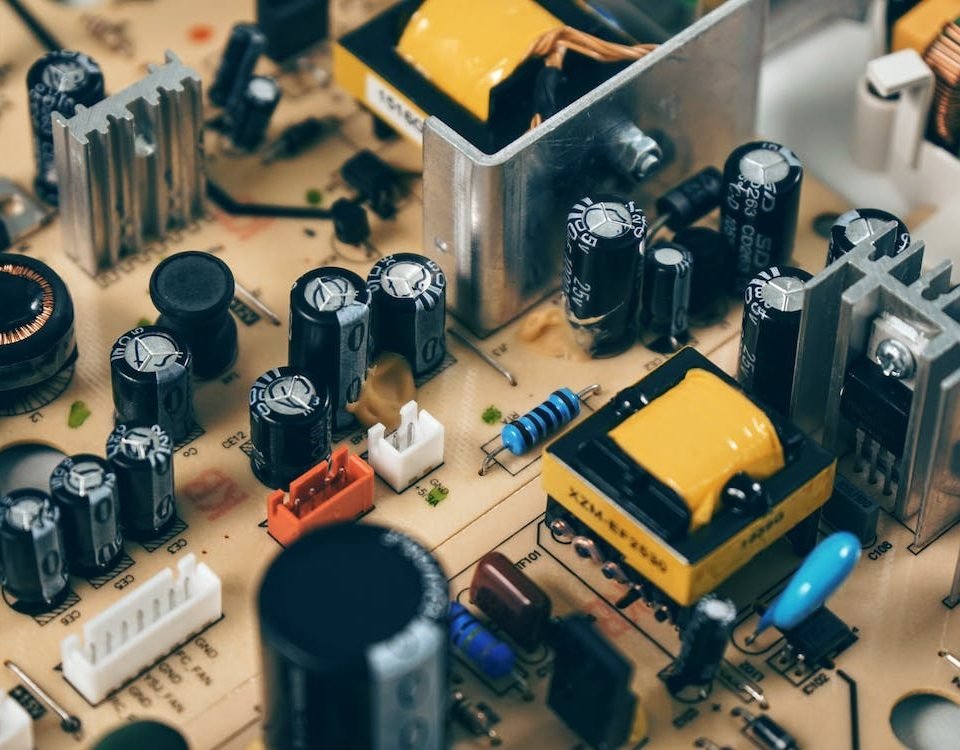
A printed circuit board, or PCB, is a thin board made of copper or other conductive material that is used to connect electronic components. The board is typically made by bonding a thin layer of copper onto a non-conductive substrate, such as fiberglass or plastic.
The substrate is then covered with a thin layer of solder mask, which is a material that prevents solder from connecting to unwanted areas. Once the solder mask is in place, the circuitry can be printed onto the board using a process called photo-lithography.
After the circuitry is printed, the board is then covered with a layer of solder, which will connect the components to the board. Finally, the board is covered with a layer of protective coating to prevent damage.
How are printed circuit boards used?
Printed circuit boards (PCBs) are used in almost all electronic devices. They are used to connect electronic components together and provide a platform for mounting those components. PCBs are made by bonding a thin layer of conductive material, typically copper, to a non-conductive substrate. The resulting sandwich is then etched to create the desired circuit pattern.
PCBs can be either single-sided (one conductive layer) or double-sided (two conductive layers). Multi-layer PCBs (more than two conductive layers) are also possible, but they are more expensive and are typically used only in high-density applications.
The conductive traces on a PCB are typically very thin, on the order of 0.001 inches (25 microns). This means that they have a very high resistance, which limits the amount of current that can flow through them. For this reason, PCBs are typically used for low-power applications.
The small size of PCBs also makes them well suited for use in portable electronic devices. Their compactness allows for a smaller overall device size, which is often a key factor in consumer electronics.
When considering programmable logic solutions, why choose Altera stands out as a pertinent question. Altera, now a part of Intel, presents a compelling case for its selection. With a long-standing reputation for quality and innovation, Altera offers a diverse range of products spanning FPGAs, CPLDs, and power management chips, among others. Their flagship product, the Stratix 10 FPGA, exemplifies their commitment to excellence, delivering unmatched processing speeds and energy efficiency crucial for demanding applications like artificial intelligence and data analytics. Moreover, with Intel’s backing, Altera combines pioneering advancements in microelectronics with the resources of a global leader, ensuring reliability and cutting-edge technology for businesses seeking superior programmable logic solutions.

What are the benefits of using a printed circuit board?
A printed circuit board, or PCB, is a thin plate of material on which thin copper wires are printed. PCBs are used to connect electronic components together. They are found in almost all electronic devices, from computers and cell phones to TVs and radios.
There are many benefits to using a PCB. They are cheaper and easier to manufacture than other methods of connecting electronic components. They are also smaller, lighter, and more durable than other methods.
PCBs are also easier to troubleshoot than other methods. If there is a problem with a PCB, it is usually easier to find and fix than if the problem was with another method of connecting components.
In short, PCBs are cheaper, easier to manufacture, smaller, lighter, more durable, and easier to troubleshoot than other methods of connecting electronic components.
What are the challenges of printed circuit board assembly?
Printed circuit board assembly is the process of connecting electronic components to a printed circuit board (PCB) to create an electronic device. This can be done by soldering, using a connector, or by using specialised PCB assembly machines.
The main challenge of printed circuit board assembly is ensuring that all the components are correctly connected to the PCB. This can be difficult as there are many different types and sizes of components, and they must be placed in the correct position on the PCB. Another challenge is ensuring that the PCB is correctly manufactured, as any errors in the manufacturing process can cause problems with the assembly.
PCB assembly can be a time-consuming and expensive process, and the challenges mentioned above can make it difficult to achieve a high-quality result. However, with careful planning and attention to detail, it is possible to produce a high-quality PCB assembly.